# JTAG
https://wiki.segger.com/JTAG
# 引脚分布
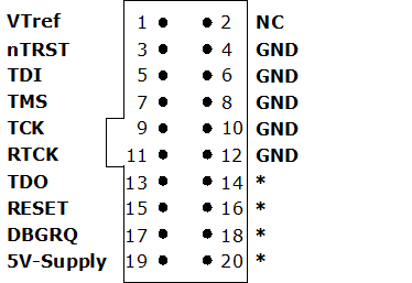
# 接口定义
| PIN | SIGNAL | TYPE | Description |
|---|---|---|---|
| 1 | VTref | Input | This is the target reference voltage. It is used to check if the target has power, to create the logic-level reference for the input comparators and to control the output logic levels to the target. It is normally fed from VDD of the target board and must not have a series resistor. |
| 2 | Not connected | NC | This pin is not connected. |
| 3 | nTRST | Output | JTAG Reset. Output from J-Link to the Reset signal of the target JTAG port. Typically connected to nTRST of the target CPU. This pin is normally pulled HIGH on the target to avoid unintentional resets when there is no connection. |
| 5 | TDI | Output | JTAG data input of target CPU. It is recommended that this pin is pulled to a defined state on the target board. Typically connected to TDI of the target CPU. |
| 7 | TMS | Output | JTAG mode set input of target CPU. This pin should be pulled up on the target. Typically connected to TMS of the target CPU. |
| 9 | TCK | Output | JTAG clock signal to target CPU. It is recommended that this pin is pulled to a defined state of the target board. Typically connected to TCK of the target CPU. |
| 11 | RTCK | Input | Return test clock signal from the target. Some targets must synchronize the JTAG inputs to internal clocks. To assist in meeting this requirement, you can use a returned, and adjusted, TCK to dynamically control the TCK rate. J-Link supports adaptive clocking, which waits for TCK changes to be echoed correctly before making further changes. Connect to RTCK if available, otherwise to GND. |
| 13 | TDO | Input | JTAG data output from target CPU. Typically connected to TDO of the target CPU. |
| 15 | nRESET | I/O | Target CPU reset signal. Typically connected to the RESET pin of the target CPU, which is typically called "nRST", "nRESET" or "RESET". This signal is an active low signal. |
| 17 | DBGRQ | NC | This pin is not connected in J-Link. It is reserved for compatibility with other equipment to be used as a debug request signal to the target system. Typically connected to DBGRQ if available, otherwise left open. |
| 19 | 5V-Supply | Output | This pin can be used to supply power to the target hardware. Older J-Links may not be able to supply power on this pin. For more information about how to enable/disable the power supply, please refer to Target power supply. |
| 4, 6, 8, 10, 12 | GND | Ground | GND pins connected to GND in J-Link. They should also be connected to GND in the target system. |
| 14, 16, 18, 20 | Res | Reserved | On some models like the J-Link ULTRA, these pins are reserved for firmware extension purposes. They can be left open or connected to GND in normal debug environment. They are not essential for JTAG or SWD in general Please do not assume them to be connected to GND inside J-Link. |
# 连接拓扑
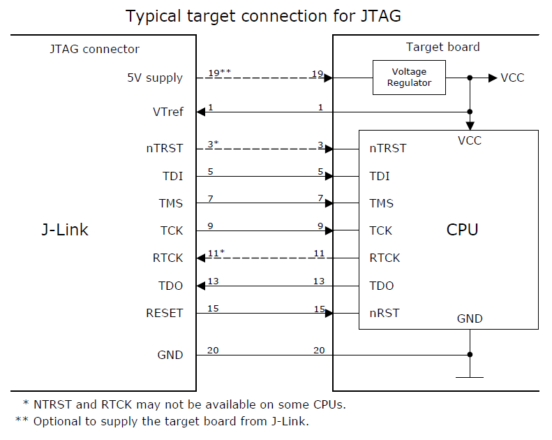
# 引脚概述
| 序号 | 引脚 | 类型 | 说明 |
|---|---|---|---|
| 9 | TCK | 输出 | 目标时钟输入引脚,为目标 CPU 提供时钟逻辑信号。 |
| 5 | TDI | 输出 | 目标数据输入引脚,用于发送串行测试指令和数据给目标 CPU。 |
| 7 | TMS | 输出 | 目标模式选择引脚,TAP (Test access port) 控制器对接收到的信号进行解码,以控制测试操作。 |
| 13 | TDO | 输入 | 目标数据输出引脚,目标 CPU 串行输出测试指令和逻辑数据。 |
| 3 | nTRST | 输出(可选) | 可选的复位输入目标引脚,用来指示 TAP 控制器的异步初始化。 |
| 11 | RTCK | 输入 | 目标 CPU 返回的时钟信号,有些目标 CPU 需要同步时钟。 |
| 15 | nRESET | 输入 / 输出 | 目标 CPU 复位信号。通常连接到目标 CPU 的 RESET 引脚。 |
# SWD
https://wiki.segger.com/SWD
# 引脚分布
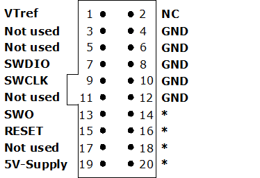
# 接口定义
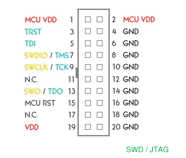
| PIN | SIGNAL | TYPE | Description |
|---|---|---|---|
| 1 | VTref | Input | This is the target reference voltage. It is used to check if the target has power, to create the logic-level reference for the input comparators and to control the output logic levels to the target. It is normally fed from VDD of the target board and must not have a series resistor. |
| 2 | Not connected | NC | This pin is not connected. |
| 3 | Not used | NC | This pin is not used by J-Link when selecting SWD as interface type. If the device may also be accessed via JTAG, this pin may be connected to nTRST, otherwise leave open. |
| 5 | Not used | NC | This pin is not used by J-Link when selecting SWD as interface type. If the device may also be accessed via JTAG, this pin may be connected to TDI, otherwise leave open. |
| 7 | SWDIO | I/O | JTAG mode set input of target CPU. This pin should be pulled up on the target. Typically connected to TMS of the target CPU. |
| 9 | SWCLK | Output | JTAG clock signal to target CPU. It is recommended that this pin is pulled to a defined state of the target board. Typically connected to TCK of the target CPU. |
| 11 | Not used | NC | This pin is not used by J-Link when selecting SWD as interface type. If the device may also be accessed via JTAG, this pin may be connected to RTCK, otherwise leave open. |
| 13 | SWO | Input | Serial Wire Output trace port. (Optional, not required for SWD communication.) |
| 15 | nRESET | I/O | Target CPU reset signal. Typically connected to the RESET pin of the target CPU, which is typically called "nRST", "nRESET" or "RESET". This signal is an active low signal. |
| 17 | Not used | NC | This pin is not connected in J-Link. |
| 19 | 5V-Supply | Output | This pin can be used to supply power to the target hardware. Older J-Links may not be able to supply power on this pin. For more information about how to enable/disable the power supply, please refer to Target power supply. |
| 4, 6, 8, 10, 12 | GND | Ground | GND pins connected to GND in J-Link. They should also be connected to GND in the target system. |
| 14, 16, 18, 20 | Res | Reserved | On some models like the J-Link ULTRA, these pins are reserved for firmware extension purposes. They can be left open or connected to GND in normal debug environment. They are not essential for JTAG or SWD in general Please do not assume them to be connected to GND inside J-Link. |
# 连接拓扑
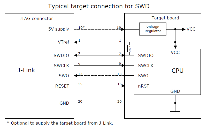
# 引脚概述
| 序号 | 引脚 | 类型 | 说明 |
|---|---|---|---|
| 9 | SWCLK | 输出 | 时钟信号引脚。 |
| 7 | SWDIO | 输入 / 输出 | 双向数据引脚。 |
| 13 | SWO | 输出(可选) | 可选的串行线跟踪输出引脚,允许 CPU 输出自定义数据,如 printf 输出,异步到 SWCLK 和其他调试引脚。 |
| 15 | RESET | 输入 / 输出 | 目标 CPU 复位信号。通常连接到目标 CPU 的 RESET 引脚。 |
# 参考
https://wiki.segger.com/20-pin_J-Link_Connector
https://developer.arm.com/documentation/101636/0100/Debug-and-Trace/JTAG-SWD-Interface
# 电路
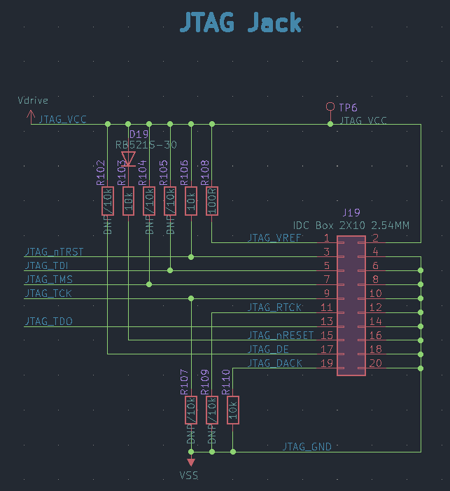
如果是要兼容 SWD,则需要在 JTAG_TMS 引脚的上拉电阻前端增加一个二极管,参照 JTAG_nRESET 上拉。
关于 J-Link 输出供电问题:
- 一次性编程器打开或者关闭
5V-Supply电源输出指令:POWER ON:一次性使能编程器电源输出。POWER OFF:一次性关闭编程器电源输出。 - 长期记录编程器打开或者关闭
5V-Supply电源输出指令:POWER ON PERM:长期打开编程器电源输出。POWER OFF PERM:长期关闭编程器电源输出。
# 附录
